IBM's Zurich Research Institute in Switzerland has developed a technology that can grow compound semiconductor crystal nanowires with almost no crystal defects on silicon components.
This can be said to be a method based on Si/CMOS technology that can improve semiconductor performance without relying on miniaturization. IBM has positioned it as a technology that can continue Moore's Law, and at the same time, it also regards it as a technology that promises to realize silicon photonics that can form optical circuits on silicon (see this site's report).
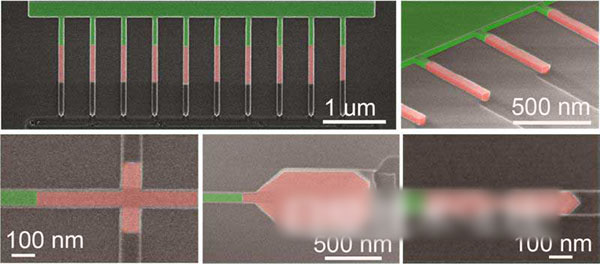
The technology developed by IBM this time is called Template-Assisted Selective Epitaxy (TASE), which is a silicon nanowire formed on a SOI (silicon-on-insulator) substrate like grafting. (NW) technology for forming a III-V compound semiconductor NW by forming a template on an SOI wafer and then, like casting, let the compound semiconductor flow into the template to grow crystals. In this year, a technology for vertically forming a compound semiconductor NW on a substrate using this TASE technology is released. This time, NW is formed on the substrate in parallel.
The method of forming the compound semiconductor NW has roughly the following steps: (1) A 25-50 nm thick silicon layer is formed on a (100) crystal plane SOI substrate, and a pattern is formed by electron beam lithography, and then formed into a shape almost equal to The resulting NW is the same silicon NW.
(2) A 30 nm thick SiO2 layer is formed on the silicon NW by atomic layer deposition (ALD). However, the top of the NW should be pre-etched using techniques such as etching to remove SiO2. Other SiO2 layers will become the template for the compound semiconductor NW.
(3) Part of the silicon NW in the template is removed from the opening of (2) by etching. The remaining silicon crystal plane becomes a (111) crystal plane. Then, crystals of the compound semiconductor are grown in the template by metal organic chemical vapor deposition (MOCVD).
(4) Etching to remove SiO2 that had previously become a template using an aqueous solution of hydrogen fluoride (HF). Through the above steps, you get an element that looks like the compound semiconductor NW is grafted onto the silicon NW.
According to related papers, the compound semiconductor NW fabricated on SOI wafers using this technology has very high crystalline quality. For example, indium arsenide (InAs) NW, the carrier mobility obtained by Hall effect measurement is up to 5400cm2/Vs at room temperature. The paper said, "This strongly proves that the manufactured NW has almost no crystal defects." The first author of the paper, Heinz Schmid, a researcher at the Zurich Research Institute in Zurich, also believes that "there is no defect is the key point that the technology is different from other technologies that allow compound semiconductor crystals to grow on silicon wafers. ". (Reporter: Nozawa Tetsuo)
LED Advertising Display,LED Display Screen,LED Advertising Screen,LED Display
SHENZHEN YGHQ Optoelectronics Co.,ltd. , https://www.leds-smd.com